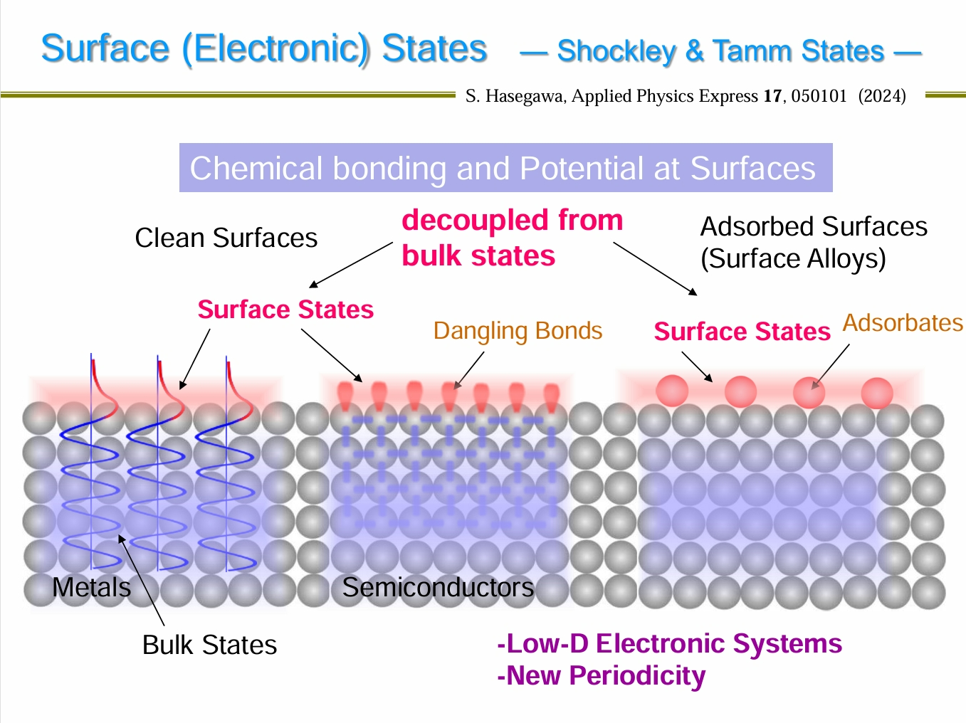
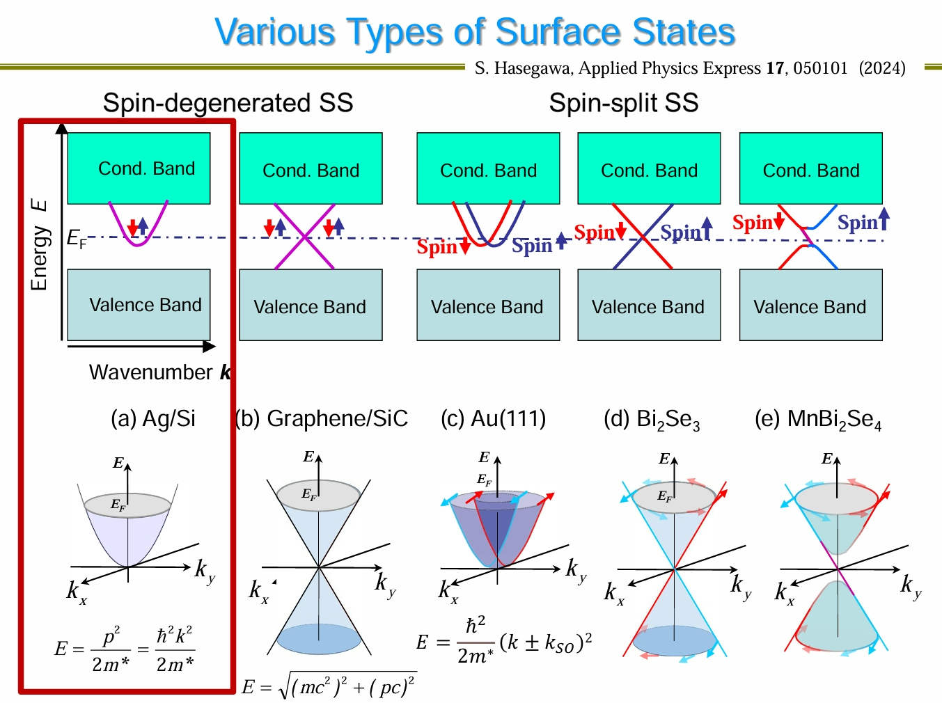
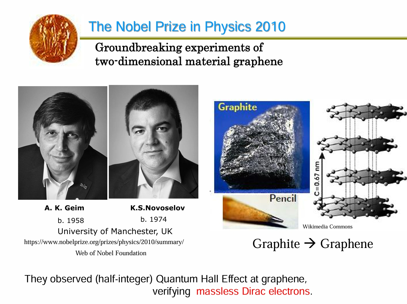
Electronic states at surfaces, interfaces, and edges of materials emerge due to different reasons and have their own characters, which are expected to be useful for intriguing physics and possible applications to electronic/spintronics devices. Especially emerging quantum materials, such as graphene and similar monatomic-layer materials, van der Waals two-dimensional crystals, and topological insulators, show prominent features in the surface/edge states. Such states at the boundaries are different from those inside the three- or two-dimensional crystals, because of the truncation of crystal lattice periodicity, space-inversion-symmetry breaking, and difference in topology in band structures across the boundaries. Such quantum materials are expected to be key ingredients for energy-saving/-harvesting technology as well as quantum computation/information technology. This is based on exotic phenomena at the states, such as spin–momentum locking of electrons, dissipation-less charge/spin currents, nonreciprocal current, and possible Majorana fermions. In this presentation, the fundamental concepts of such surface/edge states are introduced from the viewpoint of surface physics. Especially charge and spin-related transport properties are discussed based on controls of the atomic and electronic structures of materials by using state-of-the-art techniques.
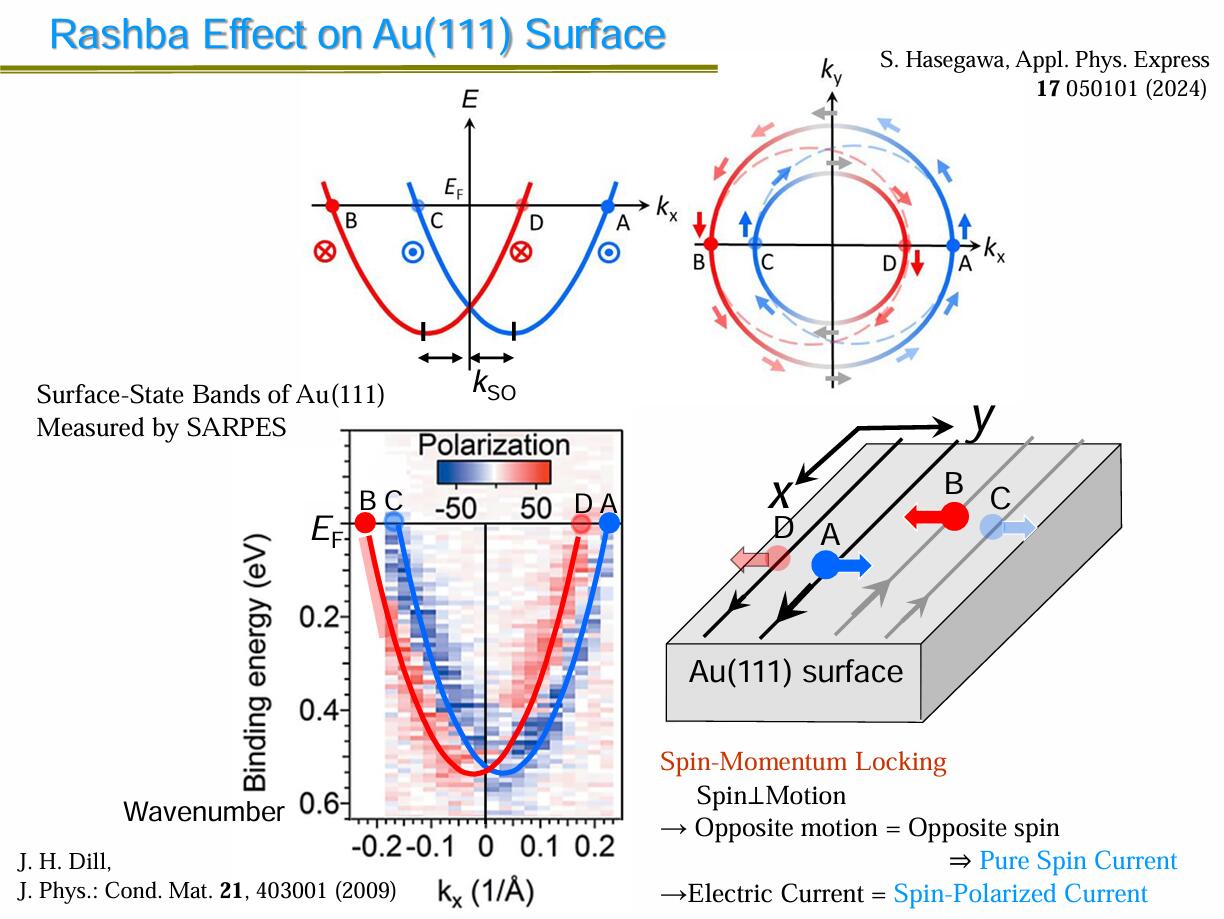
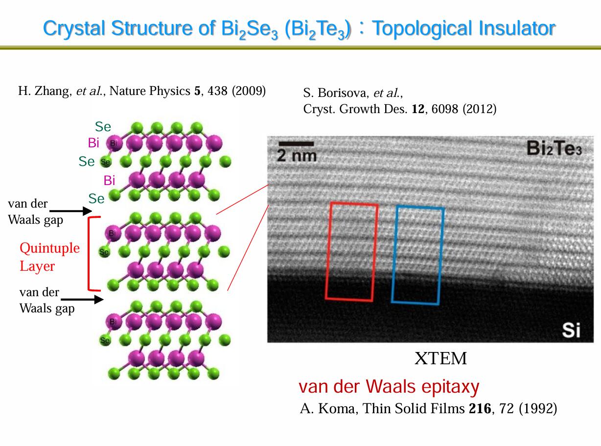
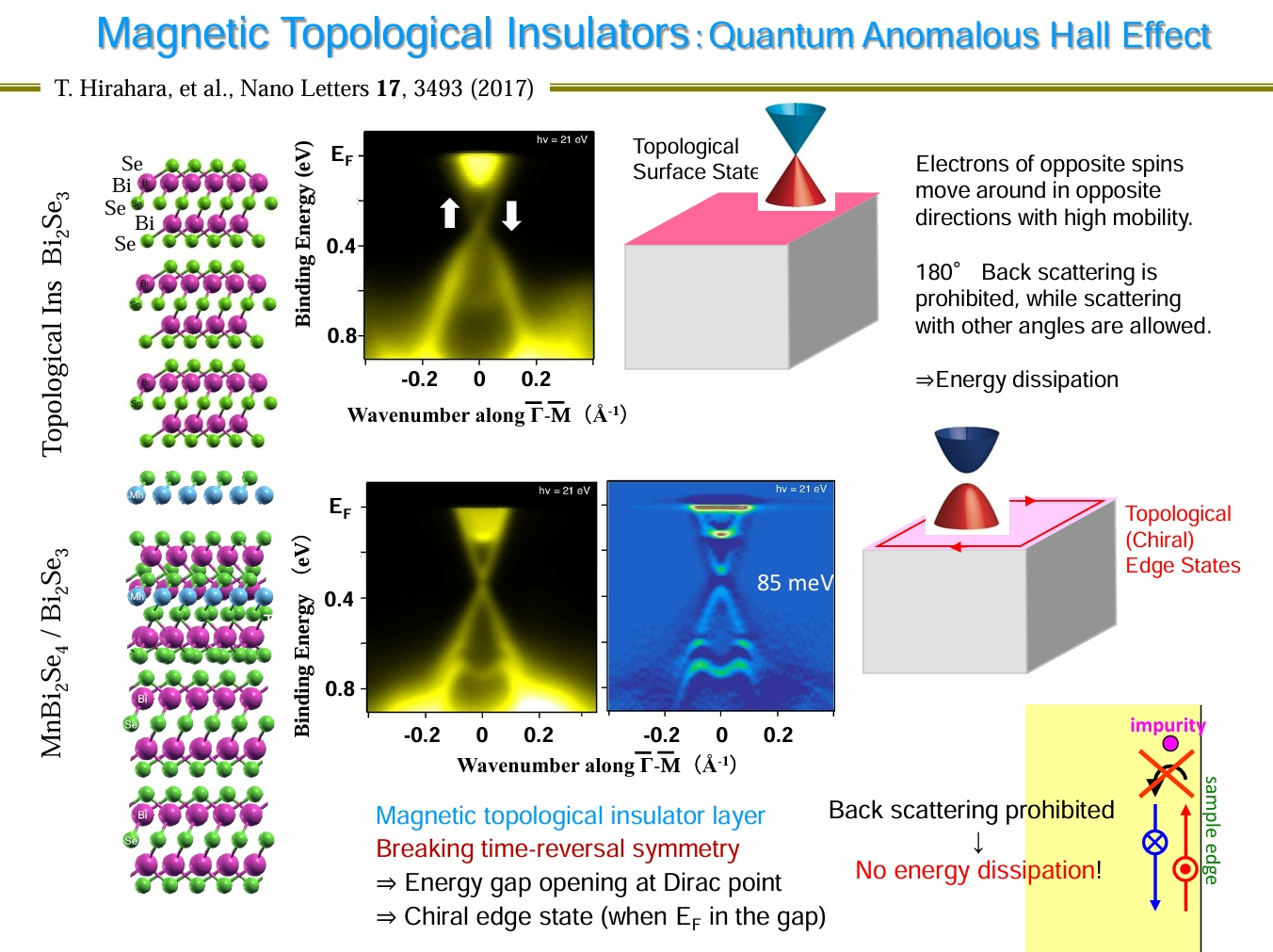
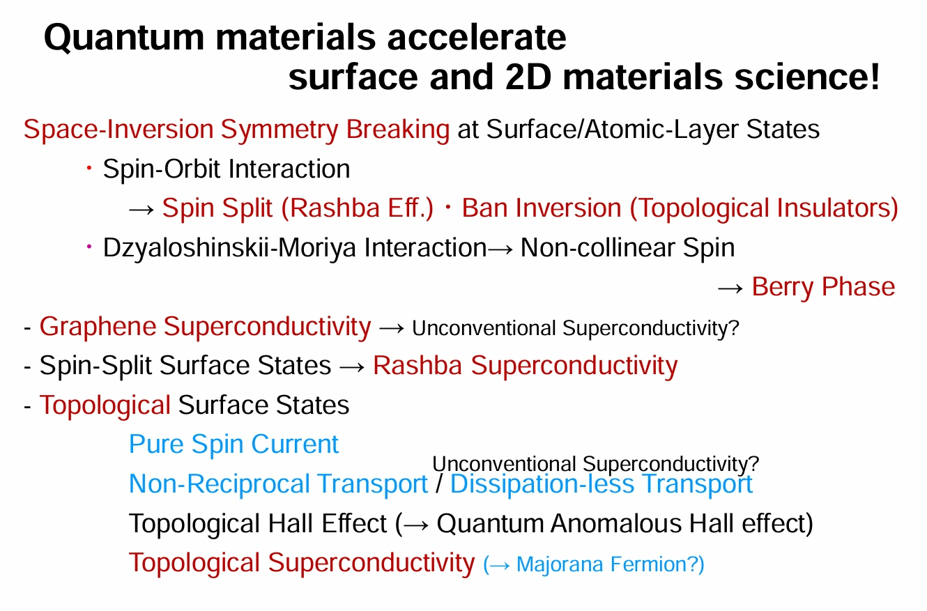
1. S. Hasegawa, Surface and interface physics driven by quantum materials, Appl. Phys. Express 17, 050101 (2024).
2. S. Hasegawa and F. Grey, Electronic transport at semiconductor surfaces––from point-contact transistor to micro-four-point probes, Surf. Sci. 500, 84 (2002).
3. H. Aizawa, M. Tsukada, N. Sato, and S. Hasegawa, Asymmetric structure of the Si(111)-3×3-Ag surface, Surf. Sci. 429, L509 (1999).
4. T. Hirahara, I. Matsuda, M. Ueno, and S. Hasegawa, The effective mass of a free-electron-like surface state of the Si(111)3×3-Ag surface investigated by photoemission and scanning tunneling spectroscopies, Surf. Sci. 563, 191 (2004).
5. C.H. Liu, I. Matsuda, R. Hobara, and S. Hasegawa, Interaction between adatom-induced localized states and a quasi-two-dimensional electron gas, Phys. Rev. Lett. 96, 036803 (2006)
6. N. Sato, S. Takeda, T. Nagao, and S. Hasegawa, Electron standing waves on the Si(111)-√3 ×√3-Ag surface, Phys. Rev. B 59, 2035 (1999).
7. N. Sato, T. Nagao, and S. Hasegawa, Two-dimensional adatom gas phase on the Si(111)- √3 ×√3 -Ag surface directly observed by scanning tunneling microscopy, Phys. Rev. B 60, 16083 (1999).
8. Y. Nakajima, S. Takeda, T. Nagao, S. Hasegawa, and X. Tong, Surface electrical conduction due to carrier doping into a surface-state band on Si(111) - √3×√3 -Ag, Phys. Rev. B 56, 6782 (1997).
9. S. Hasegawa and S. Ino, Surface structures and conductance at epitaxial growths of Ag and Au on the Si(111) surface, Phys. Rev. Lett. 68, 1192 (1992).
10. S. Hasegawa, I. Shiraki, F. Tanabe, R. Hobara, T. Kanagawa, T. Tanikawa, I. Matsuda, C.L. Petersen, T.M. Hansen, P. Boggild, and F. Grey, Electrical conduction through surface superstructures measured by microscopic four-point probes, Surf. Rev. Lett. 10, 963(2003).
11. I. Shiraki, T. Nagao, S. Hasegawa, C.L. Petersen, P. Bøggild, T.M. Hansen, and F. Hansen, Micro-four-point probes in a UHV scanning electron microscope for in-situ surface-conductivity measurements, Surf. Rev. Lett. 7, 533 (2000).
12. C.L. Petersen, F. Grey, I. Shiraki, and S. Hasegawa, Microfour-point probe for studying electronic transport through surface states, Appl. Phys. Lett. 77, 3782 (2000).
13. S. Hasegawa, I. Shiraki, T. Tanikawa, C.L. Petersen, T.M. Hansen, P. Boggild, and F. Grey, Direct measurement of surface-state conductance by microscopic four-point probe method, J. Phys. Condens. Matter 14, 8379 (2002).
14. T. Tanikawa, I. Matsuda, R. Hobara, and S. Hasegawa, Variable-temperature micro-four-point probe method for surface electrical conductivity measurements in ultrahigh vacuum, e-J. Surf. Sci. Nanotech. 1, 50 (2003).
15. I. Shiraki, F. Tanabe, R. Hobara, T. Nagao, and S. Hasegawa, Independently driven four-tip probes for conductivity measurements in ultrahigh vacuum, Surf. Sci. 493, 633 (2001).
16. S. Hasegawa, I. Shiraki, F. Tanabe, and R. Hobara, Transport at surface nanostructures measured by four-tip STM, Curr. Appl. Phys. 2, 465 (2002).
17. T. Kanagawa, R. Hobara, I. Matsuda, T. Tanikawa, A. Natori, and S. Hasegawa, Anisotropy in conductance of a quasi-one-dimensional metallic surface state measured by a square micro-four-point probe method, Phys. Rev. Lett. 91, 036805 (2003).
18. W. Norimatsu and M. Kusunoki, Transitional structures of the interface between graphene and 6H–SiC (0001), Chem. Phys. Lett. 468, 52 (2009).
19. A. Bostwick, T. Ohta, T. Seyller, K. Horn, and E. Rotenberg, Quasiparticle dynamics in graphene, Nat. Phys. 3, 36 (2007).
20. S. Ichinokura, K. Sugawara, A. Takayama, T. Takahashi, and S. Hasegawa, Superconducting calcium-intercalated bilayer graphene, ACS Nano 10, 2761 (2016).
21. Y. Cao, V. Fatemi, S. Fang, K. Watanabe, T. Taniguchi, E. Kaxiras, and P.J. Herrero, Unconventional superconductivity in magic-angle graphene superlattices, Nature 556, 43 (2018).
22. Y. Cao, V. Fatemi, A. Demir, S. Fang, S.L. Tomarken, J.Y. Luo, J.D.S. Yamagishi, K. Watanabe, T. Taniguchi, E. Kaxiras, R.C. Ashoori, and P.J. Herrero, Correlated insulator behaviour at half-filling in magic-angle graphene superlattices, Nature 556, 80 (2018).
23. J.B. Goodenough and K.S. Park, The Li-ion rechargeable battery: a perspective, J. Am. Chem. Soc. 135, 1167 (2013).
24. T.E. Weller, M. Ellerby, S.S. Saxena, R.P. Smith, and N.T. Skipper, Superconductivity in the intercalated graphite compounds C6Yb and C6Ca, Nat. Phys. 1, 39 (2005).
25. Y. Endo, X. Yan, M. Li, R. Akiyama, C. Brandl, J.Z. Liu, R. Hobara, S. Hasegawa, W.S. Wan, K.S. Novoselov, and W.X. Tang, Dynamic topological domain walls driven by lithium intercalation in graphene, Nat. Nanotechnol. 18, 1154 (2023).
26. W. Norimatsu and M. Kusunoki, Growth of graphene from SiC{0001} surfaces and its mechanisms, Semicond. Sci. Technol. 29, 064009 (2014).
27. J.S. Alden, A.W. Tsen, P.Y. Huang, R. Hovden, L. Brown, J. Park, D.A. Muller, and P.L. McEuen, Strain solitons and topological defects in bilayer graphene, Proc. Natl. Acad. Sci. U.S.A. 110, 11256 (2013).
28. N.M. Caffrey, L.I. Johansson, C. Xia, R. Armiento, I.A. Abrikosov, and C. Jacobi, Structural and electronic properties of Li-intercalated graphene on SiC(0001), Phys. Rev. B 93, 195421 (2016).
29. M. Yamada, T. Hirahara, R. Hobara, S. Hasegawa, H. Mizuno, Y. Miyatake, and T. Nagamura, Surface electrical conductivity measurement system with micro-four-point probes at sub-kelvin temperature under high magnetic field in ultrahigh vacuum, e-J. Surf. Sci. Nanotech. 10, 400 (2012).
30. H. Toyama, R. Akiyama, S. Ichinokura, M. Hashizume, T. Iimori, Y. Endo, R. Hobara, T. Matsui, K. Horii, S. Sato, T. Hirahara, F. Komori, and S. Hasegawa, Two-dimensional superconductivity of Ca-intercalated graphene on SiC: vital role of the interface between monolayer graphene and the substrate, ACS Nano 16, 3582 (2022).
31. E. Belandria, Propiedades vibracionales de nanotubos de carbono de doble pared vacíos y rellenos con Se, Te, Fe, HgTe, PbTe, CdSe y Pbl2 (Doctoral dissertation, Universidad de los Andes, Venezuela, 2008).
32. M. Orlita and M. Potemski, Dirac electronic states in graphene systems: optical spectroscopy studies, Semicond. Sci. Technol. 25, 063001 (2010).
33. G. Csányi, P.B. Littlewood, A.H. Nevidomskyy, C.J. Pickard, and B.D. Simons, The role of the interlayer state in the electronic structure of superconducting graphite intercalated compounds, Nat. Phys. 1, 42 (2005).
34. J.H. Dil, Spin and angle resolved photoemission on non-magnetic low-dimensional systems, J. Phys. Condens. Matter 21, 403001 (2009).
35. 95th Birthday of Emmanuel Rashba, Exp. Theor. Phys. 135, 387 (2022).
36. A.V. Matetskiy, S. Ichinokura, L.V. Bondarenko, A.Y. Tupchaya, D.V. Gruznev, A.V. Zotov, A.A. Saranin, R. Hobara, A. Takayama, and S. Hasegawa, Two-dimensional superconductor with a giant Rashba effect: one-atom-layer Tl-Pb compound on Si(111), Phys. Rev. Lett. 115, 147003 (2015).
37. D.V. Gruznev, L.V. Bondarenko, A.V. Matetskiy, A.A. Yakovlev, A.Y. Tupchaya, S.V. Eremeev, E.V. Chulkov, J.P. Chou, C.M. Wei, M.Y. Lai, Y.L. Wang, A.V. Zotov, and A.A. Saranin, A strategy to create spin-split metallic bands on silicon using a dense alloy layer, Sci. Rep. 4, 4742 (2014).
38. T. Nakamura, H. Kim, S. Ichinokura, A. Takayama, A.V. Zotov, A.A. Saranin, Y. Hasegawa, and S. Hasegawa, Unconventional superconductivity in the single-atom-layer alloy Si(111)−√3 ×√3 −(Tl, Pb), Phys. Rev. B 98, 134505 (2018).
39. H.J. Zhang, C.X. Liu, X.L. Qi, X. Dai, Z. Fang, and S.C. Zhang, Topological insulators in Bi2Se3, Bi2Te3 and Sb2Te3 with a single Dirac cone on the surface, Nat. Phys. 5, 438 (2009).
40. S. Borisova, J. Krumrain, M. Luysberg, G. Mussler, and D. Grützmacher, Mode of growth of ultrathin topological insulator Bi2Te3 films on Si (111) substrates, Cryst. Growth Des. 12, 6098 (2012).
41. A. Koma, Van der Waals epitaxy—a new epitaxial growth method for a highly lattice-mismatched system, Thin Solid Films 216, 72 (1992).
42. Y. Sakamoto, T. Hirahara, H. Miyazaki, S. Kimura, and S. Hasegawa, Spectroscopic evidence of a topological quantum phase transition in ultrathin Bi2Se3 films, Phys. Rev. B 81, 165432 (2010).
43. Y. Xia, D. Qian, D. Hsieh, L. Wray, A. Pal, H. Lin, A. Bansil, D. Grauer, Y.S. Hor, R.J. Cava, and M.Z. Hasan, Observation of a large-gap topological-insulator class with a single Dirac cone on the surface, Nat. Phys. 5, 398 (2009).
44. T. Hirahara, Y. Sakamoto, Y. Takeichi, H. Miyazaki, S. Kimura, I. Matsuda, A. Kakizaki, and S. Hasegawa, Anomalous transport in an 𝑛-type topological insulator ultrathin Bi2Se3 film, Phys. Rev. B 82, 155309 (2010).
45. M. Aitani, Y. Sakamoto, T. Hirahara, M. Yamada, H. Miyazaki, M. Matsunami, S. Kimura, and S. Hasegawa, Fermi-level tuning of topological insulator thin films, Jpn. J. Appl. Phys. 52, 110112 (2013).
46. D. Fan, R. Hobara, R. Akiyama, and S. Hasegawa, Inverse spin Hall effect induced by asymmetric illumination of light in topological insulator Bi2Se3, Phys. Rev. Research 2, 023055 (2020).
47. A.V. Matetskiy, I.A. Kibirev, A.N. Mihalyuk, S.V. Eremeev, D.V. Gruznev, L.V. Bondarenko, A.Y. Tupchaya, A.V. Zotov, and A.A. Saranin, Theory versus experiment for a family of single-layer compounds with a similar atomic arrangement: (Tl, X)/Si (111)√3 ×√3 (X= Pb, Sn, Bi, Sb, Te, Se), Phys. Rev. B 96, 085409 (2017).
48. T. Hirahara, S.V. Eremeev, T. Shirasawa, Y. Okuyama, T. Kubo, R. Nakanishi, R. Akiyama, A. Takayama, T. Hajiri, S. Ideta, M. Matsunami, K. Sumida, K. Miyamoto, Y. Takagi, K. Tanaka, T. Okuda, T. Yokoyama, S. Kimura, S. Hasegawa, and E.V. Chulkov, Large-gap magnetic topological heterostructure formed by subsurface incorporation of a ferromagnetic layer, Nano Lett. 17, 3493 (2017).
49. T. Takashiro, R. Akiyama, I.A. Kibirev, A.V. Matetskiy, R. Nakanishi, S. Sato, T. Fukasawa, T. Sasaki, H. Toyama, K.L. Hiwatari, A.V. Zotov, A.A. Saranin, Toru Hirahara, and S. Hasegawa, Soft-magnetic skyrmions induced by surface-state coupling in an intrinsic ferromagnetic topological insulator sandwich structure, Nano Lett. 22, 881 (2022).
The author is preparing a supplementary material as a response to the reviewers, which will be published shortly after the publication of the video article.


